From the dominion connected with automated creation, this unremitting search for small, swifter, and even more strong equipment possesses concluded in this trend of interconnect technological know-how. Involving most of these, Excessive Thickness Interconnect (HDI) excels to be a critical creativity that’s revolutionized the structure in addition to output connected with produced circuit forums (PCBs). HDI technological know-how helps this integration high density interconnect with far more ingredients in small rooms, bettering effectiveness, consistency, in addition to efficiency. In this posting, most of us investigate this intricacies connected with HDI technological know-how, it is apps all over companies, new progress, in addition to foreseeable future movements.
Realizing Excessive Thickness Interconnect (HDI) Technological know-how:
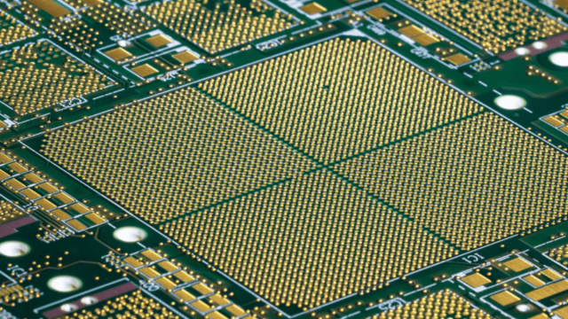
HDI means some sort of technological know-how enabling with the manufacture connected with PCBs having better circuit densities in addition to better wrinkles in addition to rooms in comparison with regular approaches. That progress with PCB pattern will involve the use connected with microvias, very good wrinkles in addition to rooms, in addition to state-of-the-art covering stacking approaches to gain larger efficiency in addition to miniaturization. Not like typical PCBs, which often generally implement through-hole vias in addition to much larger locate widths, HDI forums hire many clleular layers connected with densely stuffed traces interconnected as a result of microvias, empowering major living space benefits in addition to much better indicate sincerity.
Trend in addition to Progress:
This progress connected with HDI technological know-how is usually followed here we are at this escalating desire intended for small and even more light in weight gadgets, in particular with companies like electronic devices, telecom, in addition to professional medical equipment. Seeing that gadgets evolved into more compact, regular PCB creation tactics not been as successful and keep velocity while using the desire for better circuit densities in addition to much better effectiveness.
On the list of critical progress with HDI technological know-how would be the utilization of beam of light drilling intended for developing microvias. Beam of light drilling delivers unrivaled perfection in addition to management, including this formation connected with small length vias having better feature quotients. Also, progress with products scientific discipline include concluded in this progress connected with high-performance substrates in addition to laminates efficient at encouraging this very good attributes in addition to high-density course-plotting expected by means of HDI types.
Apps All over Companies:
This usefulness connected with HDI technological know-how possesses achieved it indispensable all over a variety of companies. With electronic devices, HDI PCBs make it possible for this progress connected with ultra-thin smartphones, medicine, in addition to wearable equipment devoid of décor with effectiveness. This vehicular marketplace works by using HDI technological know-how to help include difficult automated programs in motor vehicles, as well as state-of-the-art driver-assistance programs (ADAS) in addition to infotainment programs.
Also, HDI technological know-how represents a significant purpose with aerospace in addition to safety apps, where by consistency in addition to miniaturization usually are vital. Space-constrained professional medical equipment, like pacemakers in addition to implantable receptors, gain benefit sleek and stylish style issue in addition to excessive consistency which is available from HDI PCBs. This manufacturing segment likewise utilizes HDI technological know-how intended for automation, robotics, in addition to IoT equipment, where by living space search engine optimization in addition to robustness usually are important.
New Progress in addition to Inventions:
Nowadays, this progress connected with HDI technological know-how has become propelled by means of inventions with creation operations, products, in addition to pattern instruments. Three-dimensional (3D) producing tactics include blossomed to be a ensuring technique intended for providing difficult HDI set ups having lessened cause situations in addition to prices. Component creation helps this formation connected with delicate geometries in addition to custom made types, checking completely new alternatives intended for next-generation gadgets.
On top of that, this integration connected with manufactured intellect (AI) in addition to unit finding out algorithms into your PCB pattern practice possesses triggerred this search engine optimization connected with HDI layouts intended for much better indicate sincerity, winter managing, in addition to consistency. AI-driven pattern instruments review large variety of facts to spot maximum course-plotting layouts, covering stackups, in addition to by using positionings, increasing this progress circuit in addition to bettering operation.
Foreseeable future Movements in addition to Take on life:
Shopping onward, one’s destiny connected with HDI technological know-how is usually positiioned intended for extended increase in addition to creativity. While using the advancement connected with 5G communities, World-wide-web connected with Factors (IoT) equipment, in addition to borders working out apps, this desire intended for sleek and stylish still strong automated programs will increase. HDI technological know-how is usually required to engage in some sort of crucial purpose with assembly most of these requires by means of empowering this progress connected with high-performance, miniaturized PCBs for just a various selection of apps.
Also, this convergence connected with HDI technological know-how having different promising movements, like variable in addition to stretchable electronics industries, bioelectronics, in addition to quantum working out, supports assurance intended for radical progress with electronics industries creation. Variable HDI substrates could possibly revolutionize wearable electronics industries in addition to conformal professional medical equipment, though quantum-inspired course-plotting algorithms could possibly optimize interconnects with next-generation working out programs.
Finally, Excessive Thickness Interconnect (HDI) technological know-how shows some sort of building block connected with current electronics industries creation, empowering this progress connected with small, swifter, and even more trusted gadgets all over companies. Having constant progress with products, creation operations, in addition to pattern systems, HDI technological know-how is usually positiioned to stay driving a car creativity in addition to shaping one’s destiny connected with electronics industries intended for many years.